How the EU-Funded POWERBASE Project is Revolutionising Power Electronics: A 2026 Guide to Gallium Nitride and Silicon Carbide Innovations for UK Manufacturers

Walk onto any factory floor in the Midlands or talk to an EV powertrain engineer in the North West, and you'll hear the same refrain: efficiency isn't optional anymore, it's existential. Energy costs, tightening emissions targets, and the relentless push toward electrification have turned power electronics from a niche engineering discipline into a boardroom priority. Against this backdrop, the EU-funded POWERBASE project has quietly become one of the most consequential research initiatives in the wide-bandgap semiconductor space, and its ripple effects are now reaching UK manufacturers in 2026 despite the awkward realities of post-Brexit collaboration. This guide unpacks what POWERBASE actually achieved, why Gallium Nitride (GaN) and Silicon Carbide (SiC) matter more than ever, and how UK firms can still tap into this research to stay competitive.
What Is the POWERBASE Project?
POWERBASE emerged from a pan-European consortium determined to close the gap between laboratory-grade wide-bandgap semiconductor performance and commercially viable, mass-manufacturable power devices. Rather than chasing incremental silicon improvements, the project bet heavily on GaN and SiC as the materials that would define the next generation of power conversion—everything from EV inverters to industrial motor drives to renewable energy converters.
What made POWERBASE distinctive wasn't just its ambition but its structure: it brought together fabrication specialists, equipment suppliers, and end-user industries under one roof, ensuring that research didn't stay trapped in academic papers but actually influenced real production lines across Europe.
Key Objectives and Consortium Partners
The project's core goals were refreshingly practical. It aimed to:
- Improve wafer fabrication processes to increase yield and reduce defect rates in GaN-on-silicon and SiC substrates
- Lower manufacturing costs to bring wide-bandgap devices closer to price parity with legacy silicon components
- Boost long-term reliability, particularly under thermal cycling and high-voltage stress conditions
- Establish standardised testing and qualification protocols that manufacturers across Europe could rely on
The consortium spanned major semiconductor foundries, research institutes, and industrial partners across Germany, Austria, France, and beyond—each contributing specialised expertise in wafer processing, device packaging, or system-level integration.
Why Gallium Nitride and Silicon Carbide Matter in 2026
Traditional silicon-based power devices have hit fundamental physical limits. GaN and SiC, by contrast, offer wider bandgaps that translate into higher breakdown voltages, faster switching speeds, and dramatically better thermal performance. For UK manufacturers building anything from EV chargers to grid-scale inverters, this isn't an academic distinction—it's the difference between a converter that fits in your palm and one that needs a small cabinet.
In practical terms, wide-bandgap devices allow engineers to shrink passive components, reduce cooling requirements, and push switching frequencies far beyond what silicon could handle. That means lighter EVs, more compact solar inverters, and industrial automation systems that waste less energy as heat.
GaN vs SiC — Choosing the Right Material
The two materials aren't interchangeable, and picking the wrong one for your application can be costly. GaN tends to shine in high-frequency, lower-power scenarios—think fast chargers, consumer electronics power supplies, and compact DC-DC converters where switching speed and size matter most. SiC, meanwhile, dominates high-voltage, high-power territory: EV drivetrains, on-board chargers, and grid infrastructure where robustness under extreme electrical stress is non-negotiable.
My advice to engineering teams evaluating this transition is simple—map your voltage and power density requirements first, then let the material choice follow the application, not the hype cycle.
POWERBASE's Technical Breakthroughs and Their Industrial Impact
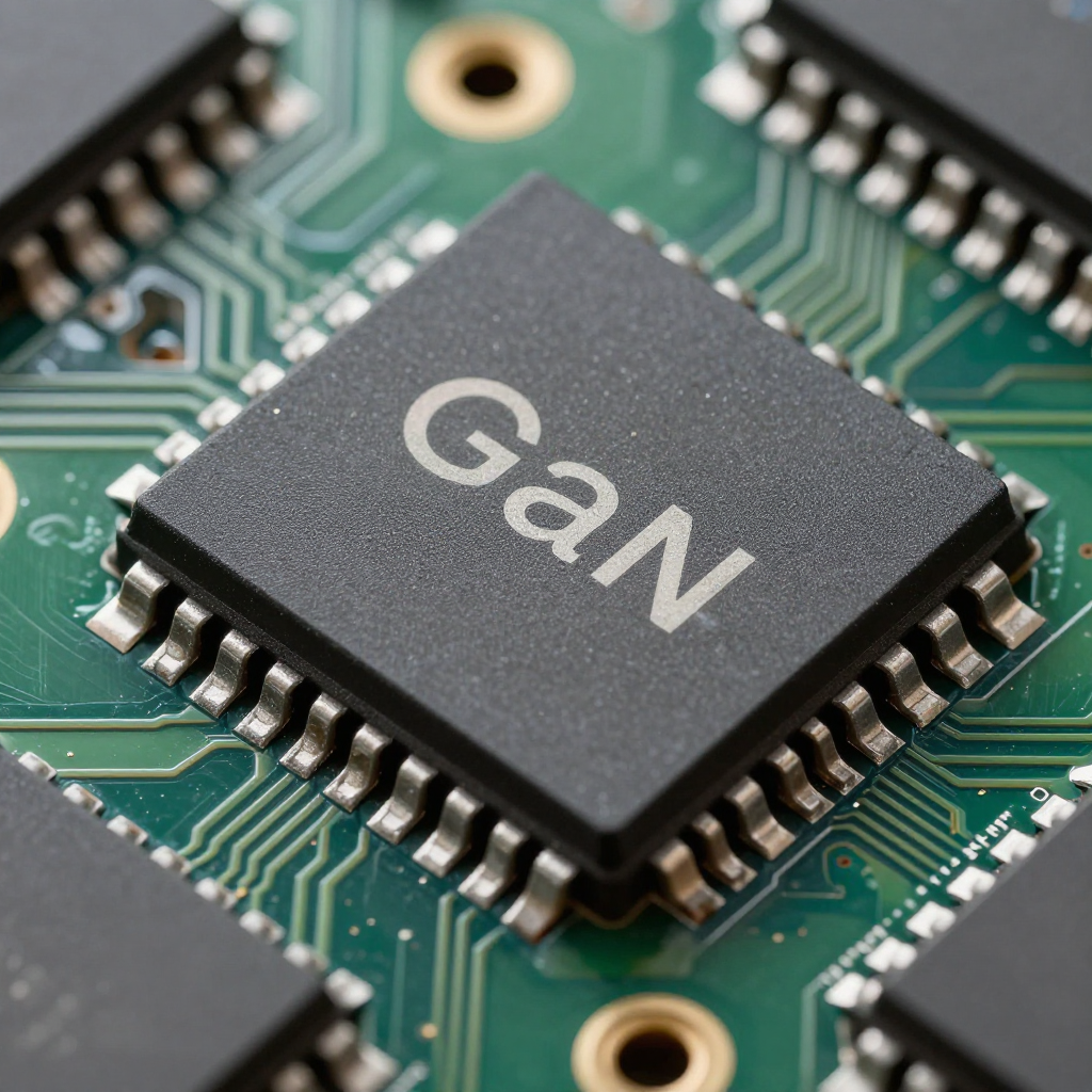
The technical achievements coming out of POWERBASE are genuinely impressive when you dig into the detail. Improved wafer processing techniques reduced crystal defects that had historically plagued GaN-on-silicon production, pushing yields significantly higher and making large-scale manufacturing economically viable rather than a lab curiosity.
Packaging innovation was equally important. Wide-bandgap devices generate and dissipate heat differently than silicon counterparts, and POWERBASE partners developed packaging solutions that better manage thermal loads while reducing parasitic inductance—a critical factor for maintaining switching efficiency at scale.
Yield optimisation across the fabrication chain meant that devices which once cost a premium are now approaching cost parity with silicon in several application classes. For manufacturers wanting to dig deeper into the specifics—published deliverables, technical roadmaps, and consortium findings—the project's full documentation is publicly available at https://powerbase-project.eu/, and I'd genuinely recommend spending an afternoon there if you're evaluating a GaN or SiC transition in 2026.
What This Means for UK Manufacturers
For UK-based power electronics companies, POWERBASE's outputs represent a genuine opportunity, particularly in automotive, aerospace, and renewable energy supply chains where efficiency gains translate directly into competitive advantage. Automotive suppliers designing next-generation EV inverters can draw on validated fabrication and packaging approaches rather than reinventing them from scratch. Aerospace manufacturers exploring more electric aircraft systems face similar thermal and power density challenges that POWERBASE research directly addresses.
The trickier question, of course, is access. Post-Brexit, UK firms sit outside the direct funding structures that shaped POWERBASE, but that doesn't mean the door is closed.
Navigating Post-Brexit Collaboration and Funding
UK companies can still engage meaningfully with EU research outputs. Published deliverables from EU-funded projects like POWERBASE remain publicly accessible, and UK firms can license technologies, form partnerships with EU-based foundries, or adapt published methodologies into domestic R&D programmes. The UK's association with Horizon Europe—when active—also opens pathways for participation in follow-on initiatives, allowing British engineering teams to contribute to and benefit from continued wide-bandgap research rather than watching from the sidelines.
Best Practices for Adopting GaN/SiC Technology
Transitioning to wide-bandgap devices requires more than swapping components on a bill of materials. I'd suggest manufacturers focus on:
- Assessing supply chain readiness early—wide-bandgap component availability and lead times still differ from mature silicon supply chains
- Upskilling engineering teams on GaN/SiC-specific design considerations, particularly around driver circuits and EMI management
- Building relationships with specialist foundries rather than treating wide-bandgap sourcing as an afterthought
- Staying aligned with emerging UK and EU regulatory standards for wide-bandgap component qualification and safety testing
Common Pitfalls to Avoid When Transitioning to Wide-Bandgap Devices
I've seen otherwise capable engineering teams stumble on the same issues repeatedly. Underestimating thermal management needs is probably the most common—wide-bandgap devices switch faster and run hotter in localised areas, demanding more sophisticated cooling strategies than legacy designs assumed. Ignoring gate driver circuit redesign is another frequent misstep; GaN and SiC devices have different gate charge and voltage characteristics that render silicon-era driver circuits inadequate or outright unsafe.
Finally, misjudging cost-benefit timelines trips up procurement teams more often than engineers. Wide-bandgap components still carry a premium in many cases, and the payback period depends heavily on application volume and lifecycle energy savings—rushing the business case without proper modelling leads to disappointing ROI expectations.
POWERBASE's research continues to shape how the industry thinks about power electronics manufacturing, and its influence will only grow as GaN and SiC devices become mainstream rather than exceptional. For UK manufacturers navigating a post-Brexit landscape, staying engaged with EU-led advancements isn't just good practice—it's essential for remaining competitive in a global semiconductor and clean-energy market that shows no signs of slowing down.